- Home
- News
- Spotlight on Science
- 3D imaging of ordered...
3D imaging of ordered domains in an Fe-Al alloy by Bragg ptychography
29-01-2019
Iron-aluminium alloys are used in industry for applications requiring high strength to weight ratio and good corrosion resistance. Within an Fe-Al alloy, anti-phase domain structures were imaged three-dimensionally by X-ray Bragg ptychography. The location of domain walls correlates strongly with the regions of maximum lattice strain, especially when the anti-phase domain wall is in a direction that requires rearrangements of atoms beyond nearest-neighbours.
Intermetallic alloys are essential in the world due to their widespread applications, e.g. in steel, in aeronautics, and the refining industries. Iron-aluminum alloys have attractive physicochemical properties, e.g. remarkable oxidation resistance and rich magnetic properties [1] and novel Fe-Al nanotwinned alloys combine lightweight with steel-like strength [2]. Depending on composition and temperature, binary alloys display several chemically-ordered phases and the macroscopic properties can be strongly affected. However, a deeper understanding of the ordered phases is missing because of limitations in currently available microscopes.
In this work, the anti-phase domain (APD) structures of an Fe-Al alloy was visualised in three dimensions by X-ray Bragg ptychography [3]. With the same technique, the general lattice strain was also accessible so it could be compared with the retrieved APD structure. A key point of the experiment was to measure both a fundamental Bragg reflection and a superlattice reflection of the exact same crystal grain. The superlattice peak is sensitive to both APD walls and general lattice strain while the fundamental reflection is only sensitive to strain. Combining information from the two measurements thus provides a unique possibility to separate those effects and independently visualise APDs and strain.
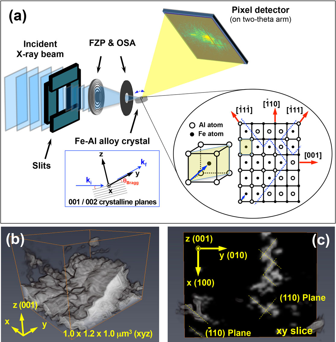
The experiment was performed at beamline ID01 with a nano-focused beam of ~170 x 80 nm2 (Figure 1a). Both the (001) superlattice and the (002) fundamental peaks were measured on the same crystallite and the data reconstructed. By subtracting the phase variations of the (002) peak from those of the (001) peak, a three-dimensional APD image was obtained (Figure 1b). The phase domain walls emerge if like elements are nearest neighbours and consequently occur preferentially on (110) planes and appears as 45° tilted structures in x-y slices like in Figure 1c.
 |
|
Figure 1. (a) Sketch of the Bragg ptychography setup at ID01. A Fresnel Zone plate (FZP) with an order-sorting aperture (OSA) provided a nanofocused beam on the sample. A MAXIPIX detector captured coherent diffraction images for different translational and rotational offsets of the Fe-Al crystal around the (001) and (002) reflections. The inset illustrates the chemically-ordered phase where the atoms order on sub-lattices with Fe (Al) occupying the centre (corner) of the bcc unit cell. The (001) peak is usually forbidden in the bcc structure but emerges due to the sub-lattice ordering. The two-fold degeneracy in choice of sub-lattice results in domain walls (blue dashed lines) where nearest-neighbour atoms are of same kind. (b) 3D rendering of antiphase domain (APD) structure after ptychographic reconstruction of the data. The filled volume corresponds to one phase, the empty volume to its antiphase with a domain wall in-between. (c) An x-y slice of the APD image in (b). The axis arrows in (b)-(c) are 250 nm long. |
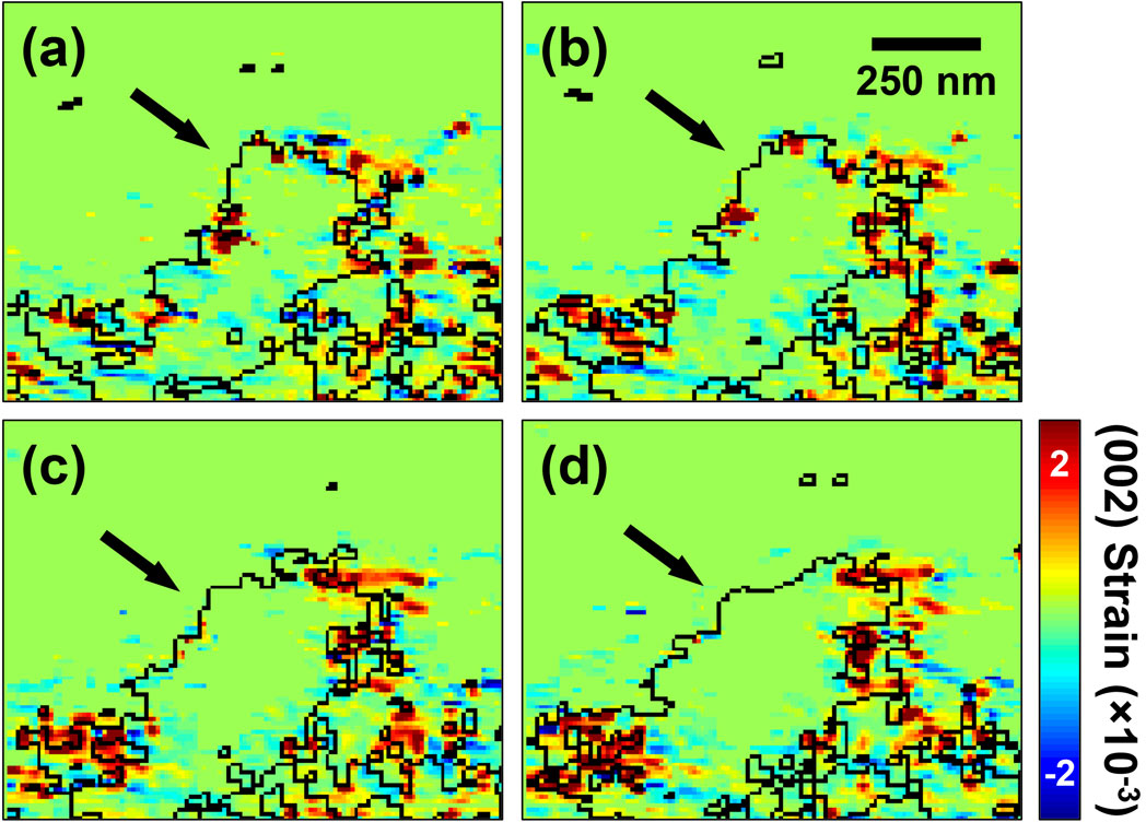
Figure 2 shows a series of 2D cross sections (y-z plane) through the phase image reconstructed from the (002) fundamental reflection. This reflection is insensitive to the APD structure and only measures the bcc lattice where a large phase shift is indicative of lattice strain, defects or tilts. On top of the images, the location of the APD wall is indicated by a black line and the correlation is obvious. The arrows point to a part of the wall that runs approximately in the (110) direction defined by nearest-neighbour atoms of similar kind. In this case, the strain is small in the wall region and hence it cannot be used as a unique identifier of where an APD wall might occur.
 |
|
Figure 2. A series of 2D cuts (20 nm separation along x) through the reconstructed phase from the (002) fundamental reflection. A high phase value indicates strong crystal lattice strain or defects. The black line outlines the location of the APD wall corresponding to sections through Fig. 1b. Obviously, in most cases there is a strong overlap between the regions of large lattice strain and the position of the APD wall. When the APD wall is approximately in the 45° direction, i.e. occurring on (110) planes, the lattice strain can, however, be less prominent (arrow in a-d). |
The next generation of diffraction-limited synchrotron sources promise to deliver 10-100 times more coherent flux than today and will allow visualisation of domain walls and strain with near-atomic resolution.
Principal publication and authors
Three-dimensional imaging of phase ordering in an Fe-Al alloy by Bragg ptychography, C. Kim (a), V. Chamard (b), J. Hallmann (a), T. Roth (a,c), W. Lu (a), U. Boesenberg (a), A. Zozulya (a), S. Leake (c), A. Madsen (a), Physical Review Letters 121, 256101 (2018); doi: 10.1103/PhysRevLett.121.256101.
(a) European X-ray Free Electron Laser Facility, Schenefeld (Germany)
(b) Aix-Marseille University, CNRS, Centrale Marseille, Institute Fresnel, Marseille (France)
(c) ESRF
References
[1] F. Plazaola et al., in Advanced Magnetic Materials edited by L. Malkinski (InTech, London, 2012), p. 133.
[2] Q. Li et al., Adv. Mater. 30, 1704629 (2018); doi: 10.1002/adma.201704629.
[3] P. Godard et al., Nature Communications 2, 568 (2011); doi: 10.1038/ncomms1569.
partners


European Synchrotron Radiation Facility - 71, avenue des Martyrs, CS 40220, 38043 Grenoble Cedex 9, France.