- Home
- News
- General News
- #worldenvironmentday...
#worldenvironmentday Perovskites, the rising star for energy harvesting
05-06-2018
Perovskites are promising candidates for photovoltaic cells, having reached an energy harvesting of more than 20% while it took silicon three decades to reach an equivalent. Scientists from all over the world are exploring these materials at the ESRF.
Photovoltaic (PV) panels exist in our society since several years now. The photovoltaic market is currently dominated by wafer-based photovoltaics or first generation PVs, namely the traditional crystalline silicon cells, which take a 90% of the market share.
Although silicon (Si) is an abundant material and the price of Si-PV has dropped in the past years, their manufacturing require costly facilities. In addition, their fabrication typically takes place in countries that rely on carbon-intensive forms of electricity generation (high carbon footprint).
But there is room for hope. There is a third generation of PV: those based on thin-film cells. These absorb light more efficiently and they currently take 10% of the market share.
One of these emerging thin-film PV cells are perovskites, with a chemical formula ABX3, where 'A' and 'B' are two cations of very different sizes, and X is an anion that bonds to both. In contrast with the orderly arrangement of silicon, the polycrystalline and “dirty” perovskites have started to take a prominent role in photovoltaic research.
Pros and cons of perovskites
Perovskites are very cheap, easy to synthesize and manufacture and display promising properties, namely light absorption, charge-carrier mobilities and lifetime. “It is a completely imperfect material, so the fact that it has such outstanding properties is really quite surprising”, explains Stephanie Pouget, scientist at CEA working in this field and user at ID01. There are several different kinds of perovskites. The most studied perovskites are the so-called “MAPI” (methylammonium lead iodide). However, the best efficiencies have been obtained from more complex formulations, such as those containing formamidinium with multiple cations and mixed halide anions.
 |
|
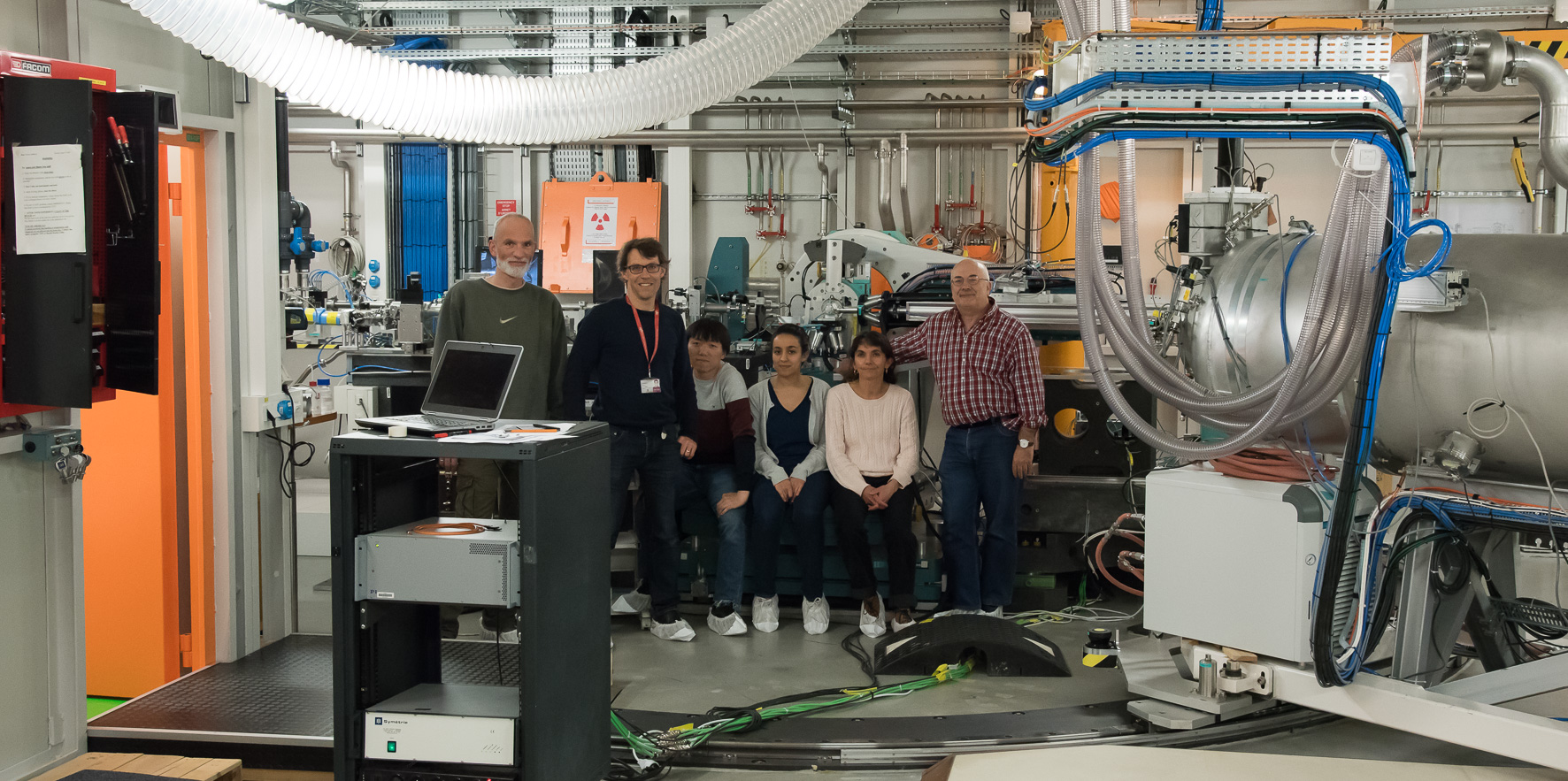
The CEA-CNRS team on ID01. From left to right: Peter Reiss, from CEA-Grenoble/INAC, Tobias Schulli from ID01, Tao Zhou from ID01, Asma Aicha Medjahed, Stephanie Pouget (both from CEA-Grenoble/INAC) and David Djurado, from the CNRS. Credits: C. Argoud. |
Perovskites can be tailored to absorb various wavelengths of light, which lets them convert more of the sunlight into electricity. In the last decade, the efficiency of these materials has reached around 23%, whilst it took silicon 30 years to reach similar performances.
There are, however, some challenges. The main issues are durability, production cost, and efficiency. There is also an environmental obstacle: perovskites currently contain lead, which, as a toxic material, would need to be replaced should the technology be used widely. “We are studying substitutes of lead, as are many other teams worldwide”, explains Peter Reiss, leader of the CEA perovskite’s team. This requires deep insight into the structure and function of the perovskite layers.
Another challenge is the improvement of the long-term stability of perovskite solar cells, currently limited to less than around1000 h, limited by degradation arising from the used device architecture (e.g. contact materials) and/or from the tendency of perovskites to rapidly deteriorate in the presence of moisture.
Unique tool for the perovskite race
Today there is a worldwide race of scientific teams working on solving these problems. “In the last five years there has been an increasing number of teams focused on this”, explains David Djurado, from the CEA-CNRS team. “The interests are so high and the development is so quick that it is almost difficult to keep up”, he says. “But we have the ESRF. On ID01 we can do experiments that are impossible to do elsewhere, so we feel that we are contributing a lot to the advance of the field”, he adds.
The CEA team has already used ID01 several times to investigate in situ the crystallisation processes of hybrid perovskites, revealing the influence of the underlying layer on the perovskite film microstructure. The team is now focussing on the ionic migration, which has been suggested to explain the J-V hysteresis effect observed for different cell architectures. Full field diffraction X-ray microscopy on ID01 is an ideal tool as it allows the operando investigation of localized structural evolutions, on a large area of the sample surface. Local accumulation of ions can be identified by imaging the dark field signal of MAPI and secondary phases and mapping the locally strained areas under different bias. A detailed understanding of the ionic migration processes is essential to better control their influence on the cell properties and pave the way for enhanced performances.
It is not only the ID01 beamline that can take credit for doing state-of-the-art research on photovoltaic cells. The XMaS Beamline (BM28) has a long-term collaboration with a team lead by Samuele Lilliu which comprises many universities — University of Sheffield, University of Cambridge, Cardiff University, University of Oxford, University of Warwick, the Khalifa University of Science and Technology (formerly Masdar Institute, United Arab Emirates) —. “We have been working together since 2014 on the development of a set-up for photovoltaics research on the beamline”, explains Oier Bikondoa, scientist on the beamline and part of the team. “Now, thanks to this development, scientists can carry out in situ measurements of solar cells based on perovskites”, he adds.
 |
|
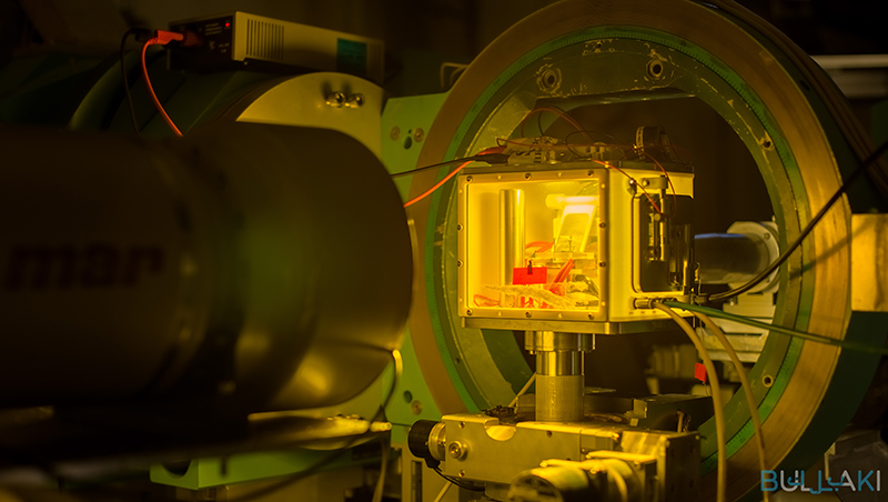
Picture of the setup at XMaS beamline for in-situ GI-WAXS and opto-electrical measurements of perovskite solar cells. Copyright: Samuele Lilliu. |
“Back in 2009, with Professor Emyr Macdonald and the XMaS team we built a chamber for studying in real-time how films for organic solar cells evolve during processing (annealing). In 2014, we started developing a new chamber with Oier Bikondoa and my team at Masdar Institute, for real-time combined structural and opto-electrical measurements of films for perovskite solar cells.”, explains Samuele Lilliu.
“Between 2015 and 2016, by exploiting a new type of device architecture for perovskite solar cells we were able to perform simultaneous in-situ grazing incidence wide angle x-ray scattering (GI-WAXS) and in-operando current-voltage measurements on metal-halide perovskite solar cells, and show how the remarkably clean semiconductor behaviour of perovskites films emerges in the earliest phase of conversion from the as-coated precursor film”, he adds
GI-WAXS measurements can provide average information of the perovskite crystallites during their formation thanks to the large footprint of the X-rays. However, these X-ray beams are not small enough for understanding how the structural properties of the perovskite material vary across the sample. In parallel with the measurements at XMaS, Lilliu’s team has been working with Manfred Burghammer’s team at ID13 on the characterization of the local structure of perovskite films by scanning nanofocus X-ray diffraction (nXRD). With nXRD, they were able to perform grain segmentation and extract the lateral size, strain and orientation of individual perovskite platelets, and they combined this with other local opto-electrical and chemical measurements to shed new light on the presence and influence of structural defects in halide perovskites .
“We look forward to the inauguration of the upgraded ESRF and hope to continue adding knowledge that will contribute to further understanding of the working mechanisms of these materials”, he concludes.
On the market
The question as to when perovskites will be widely available as photovoltaic cells does not seem to have an answer just yet. Thanks to the current promising research, scientists believe their application will expand to other fields, including micro- and nanoelectronics and battery and energy storage.
Text Montserrat Capellas Espuny
References:
Bouchard M., et al, Journal of Physical Chemistry C, vol.121, p.7596-7602, 2017.
http://www.esrf.fr/sites/www/home/news/spotlight/content-news/spotlight/spotlight310.html
http://www.esrf.fr/home/news/spotlight/content-news/spotlight/spotlight271.html
Top image: A specimen with perovskites crystals from Arkansas (USA). Credits: Rob Lavinsky, iRocks.com.
partners


European Synchrotron Radiation Facility - 71, avenue des Martyrs, CS 40220, 38043 Grenoble Cedex 9, France.